
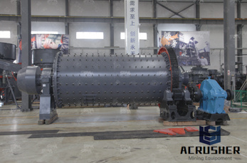
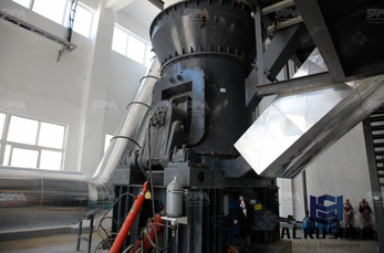
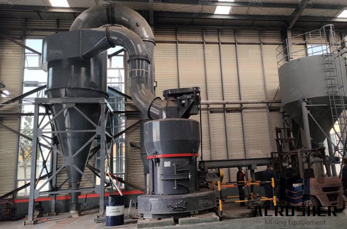
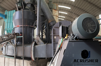
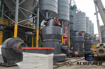
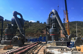
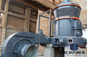
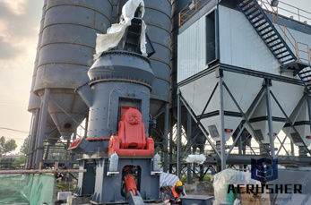
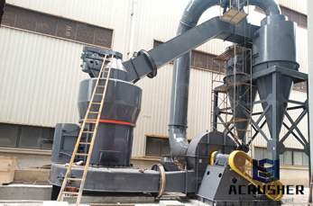
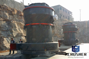
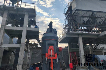
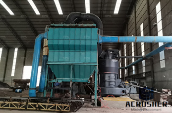
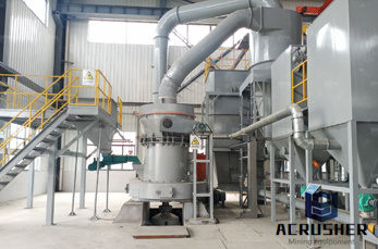
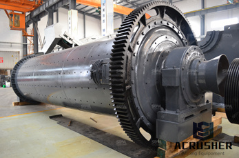
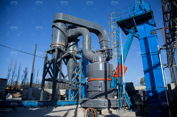
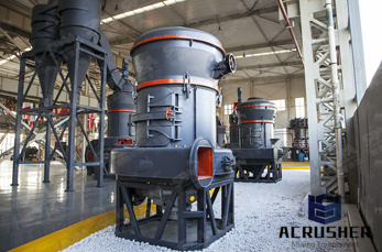
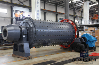
grinding process of silicon manufacturer Grasping strong production capability, advanced research strength and excellent service, Shanghai grinding process of silicon supplier create the value and bring values to all of customers.
 WhatsApp)
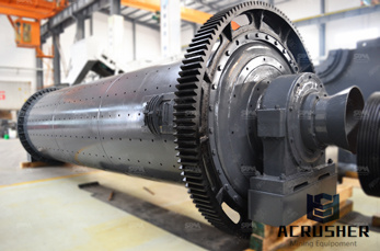
Our silicon wafer manufacturing process can be divided into two stages, namely, pulling single crystal ingots and slicing and polishing the silicon wafers. Poly-Crystaline Silicon (Nuggets) ... Various types of grinding stones are used to shape wafer edge to meet Costomers' unique edge shape.
Syagrus Systems uses the 3M Wafer Support System to meet the demands of today's technology companies for extremely thin silicon wafers and die used in complex applications. We have over 15 years of silicon wafer thinning and wafer backgrinding experience, including bumped wafer backgrinding and have provided wafer backgrind services since 1997.
This study investigates warping of silicon wafers in ultra-precision grinding-based back-thinning process. By analyzing the interactions between the wafer and .
Silicon carbide: Silicon carbide grinding wheels are made by mixing pure white quartz, petroleum coke and small amounts of sawdust and salt, and then by firing the mixture in an electric furnace. The process is called synthesizing the coke and sand.
circuits is grinding process. Grinding is done to reduce the thickness and improve the surface quality of the wafer at a high throughput. Hence, its use in wafer manufacturing is increasing. Grinding is finding some newer applications in the manufacturing process such as partially replacing lapping and polishing operations.
Oct 22, 2019· The Process. The process of thinning wafers involves using a mechanical grinding wheel, chemical slurry, and IR equipment- to help you measure the thickness. A classic grinding process would involve three stages: coarse grinding, fine grinding, and polishing. For example, you want to grind a silicon wafer from 725 micrometers to 50 micrometers.
This review paper discusses historical perspectives on grinding of silicon wafers, impacts of wafer size progression on applications of grinding in silicon wafer manufacturing, and interrelationships between grinding and two other silicon machining processes (slicing and polishing). It is organized into six sections.
Back grinding is a process that removes silicon from the back surface of a wafer. Silicon Valley Microelectronics provides grinding on our own substrates or on customer supplied wafers. We process bare and device patterned wafers with high yield and offer wafer thinning to customer specifications. SVM Wafer Back Grinding Capabilities:
development of fine grinding of silicon wafers, a large amount of research work is needed. As the first of a series of papers dealing with fine grinding of silicon wafers, this paper reports and discusses some experimental work on the effects of grinding wheels, process parameters and grinding coolant.
side grinding of silicon wafers: a review and analysis of experimental investigations," Machining Science and Technology, Vol. 13, No. 3, pp. 285-316. Abstract . Simultaneous double side grinding (SDSG) has become an important flattening process for manufacturing of 300 mm silicon wafers. However, the literature contains only a small number of
on the effects of grinding wheels, process parameters and grinding coolant. As a follow-up, this paper reports a designed experimental study on fi ne grinding of silicon wafers. Three-factor two-level full factorial design is used in this study. The objective is to reveal the main effects as well as the interaction effects of three process
Mechanically thinning the silicon substrate is generally required at two stages of main stream semiconductor manufacture process. One is slicing the silicon ingot, the other is wafer back grinding after circuit process is completed. (Various CMP s...
This review paper discusses historical perspectives on grinding of silicon wafers, impacts of wafer size progression on applications of grinding in silicon wafer manufacturing, and interrelationships between grinding and two other silicon machining processes (slicing and polishing). It .
From observations of individual grinding scratches and an analysis of the experimental results, it is concluded that virtually all of the grinding energy is expended by viscous deformation. Material removal occurs by flow into chips with silicon carbide abrasive and by brittle fracture preceded by viscous deformation with diamond abrasive.
The latest state of the art in grinding technology are double side grinding machines. Both sides of a wafer are ground at the same time. These machines have a high performance in flatness, roughness and throughput and can replace the lapping process completely - sometimes even the etching process.
Wafer backgrinding is a semiconductor device fabrication step during which wafer thickness is reduced to allow stacking and high-density packaging of integrated circuits (IC).. ICs are produced on semiconductor wafers that undergo a multitude of processing steps. The silicon wafers predominantly used today have diameters of 200 and 300 mm. They are roughly 750 μm thick .
Dec 15, 2000· Silicon carbide is an abrasive used for grinding gray iron, chilled iron, brass, soft bronze and aluminum, as well as stone, rubber and other non-ferrous materials. Ceramic aluminum oxide is the newest major development in abrasives. This is a high-purity grain manufactured in a gel sintering process.
Fine grinding of silicon wafers: designed experiments. on the effects of grinding wheels, process parameters and grinding coolant. As a followup, this paper reports a designed experimental study on fi ne grinding of silicon wafers. Threefactor twolevel full factorial design is used in this study.
Back grinding is a process that removes silicon from the back surface of a wafer. Silicon Valley Microelectronics provides grinding on our own substrates or on customer supplied wafers. We process bare and device patterned wafers with high yield and offer wafer thinning to customer specifications. SVM Wafer Back Grinding Capabilities:
Jun 15, 2018· Fine rotation grinding (FRG) is a typical efficient method for silicon mirror manufacture. A geometric model is developed in this paper to research silicon mirror surface figure control mechanism in FRG process. The model demonstrates the relationship between the grinding spindle obliquity and the mirror surface figure.
Norton Abrasives - St. Gobain 37C (07660710466) Grinding Wheel Dressing Stick, Medium Grit Silicon Carbide Abrasive for Cleaning, Opening and Reshaping Grinding .
Subsurface damage (SSD) induced by silicon wafer grinding process is an unavoidable problem in semiconductor manufacturing. Although experimental attempts have been made on investigation of the influential factors on the SSD depth, however, few theoretical studies have been conducted to obtain SSD depth through grinding parameters.
Dec 23, 2018· This process is known as Dressing of grinding wheel and the whole process takes 15 to 20 minutes to operate. The life of the grinding wheel is described as the time period between two successive dressings. Grinding operation is one of the machining processes which consume the highest specific cutting energy with very less material removal rate.
Silicon Carbide (SiC) is a synthetic mineral most commonly produced in electrical resistance furnaces, by the Acheson process, named after the American E.G. Acheson who invented it in 1891.
WhatsApp)